 Laboratory of Statistical Thermodynamics and Macromolecules
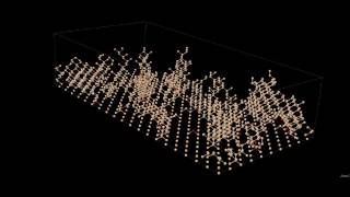
Hierarchical simulation of microcrystalline PECVD silicon film growth and structure
Plasma enhanced chemical vapor deposition (PECVD) is a popular technique for growing Si films. The high growth rates obtained by exploiting the presence of reactive radicals in the gas phase render this technique of industrial interest, since it allows for the fast deposition of thin films even at moderately low temperatures, since no thermal cracking is required. By tuning the growth parameters, PECVD can be used to grow epitaxial, amorphous, and micro- (μc) or nanocrystalline (nc) films. Being promising for the production of solar cells with a good efficiency/cost ratio, nc-Si films have attracted recently wide attention. Our goal here is to design and implement hierarchical simulation methodologies for the study of PECVD of silicon films, the emphasis placed on the elucidation of the microscopic mechanisms as well as the interplay between atomic level and macroscopic design parameters associated with the development of nano- or micro-scale crystalline regions in the grown layer. The ultimate goal is to use multi-scale modeling as a design tool for tackling the issue of local crystallization depending on the environment, thus also of the growth parameters.
Our simulation approach is based on the design of a very efficient, large-scale kinetic Monte Carlo (kMC) algorithm capable of generating samples of representative Si films based on a validated chemistry model. In a second step, the generated film is subjected to an atomistic simulation study restoring the molecular details lost or ignored in the kMC model and tuning the local structure i.e. the important morphological details associated with the presence of crystalline and amorphous regions (and the intervening interfacial domains) in the grown film. The kMC method is based on a carefully chosen set of reacting or active radicals (species) in the gas phase impinging the film and a detailed set of surface reactions. For a three-dimensional Si(001)-(2x1):H crystalline lattice, our kMC method allows us to study several seconds of film growth, resulting in thicknesses in the order of tenths of nanometers. The kMC method has been validated by carrying out computational experiments over a wide range of dilution ratios and by comparing the numerical results for the growth rate and roughness with the corresponding experimental data; very good agreement is observed in most cases. In a final step, the 3-d structures generated with kMC are used as input in large-scale MD simulations for times up to several microseconds to allow the system further relax towards the preferred morphological state at the conditions of interest. This allows us to obtain predictions for other industrially relevant quantities and observables (e.g. hydrogen content and crystallinity which are experimentally accessible by FTIR and Raman spectroscopy), thus opening the way to fully understanding the underlying complex molecular mechanisms responsible for the growth of micro- or nanocrystalline films.