 Laboratory of Statistical Thermodynamics and Macromolecules
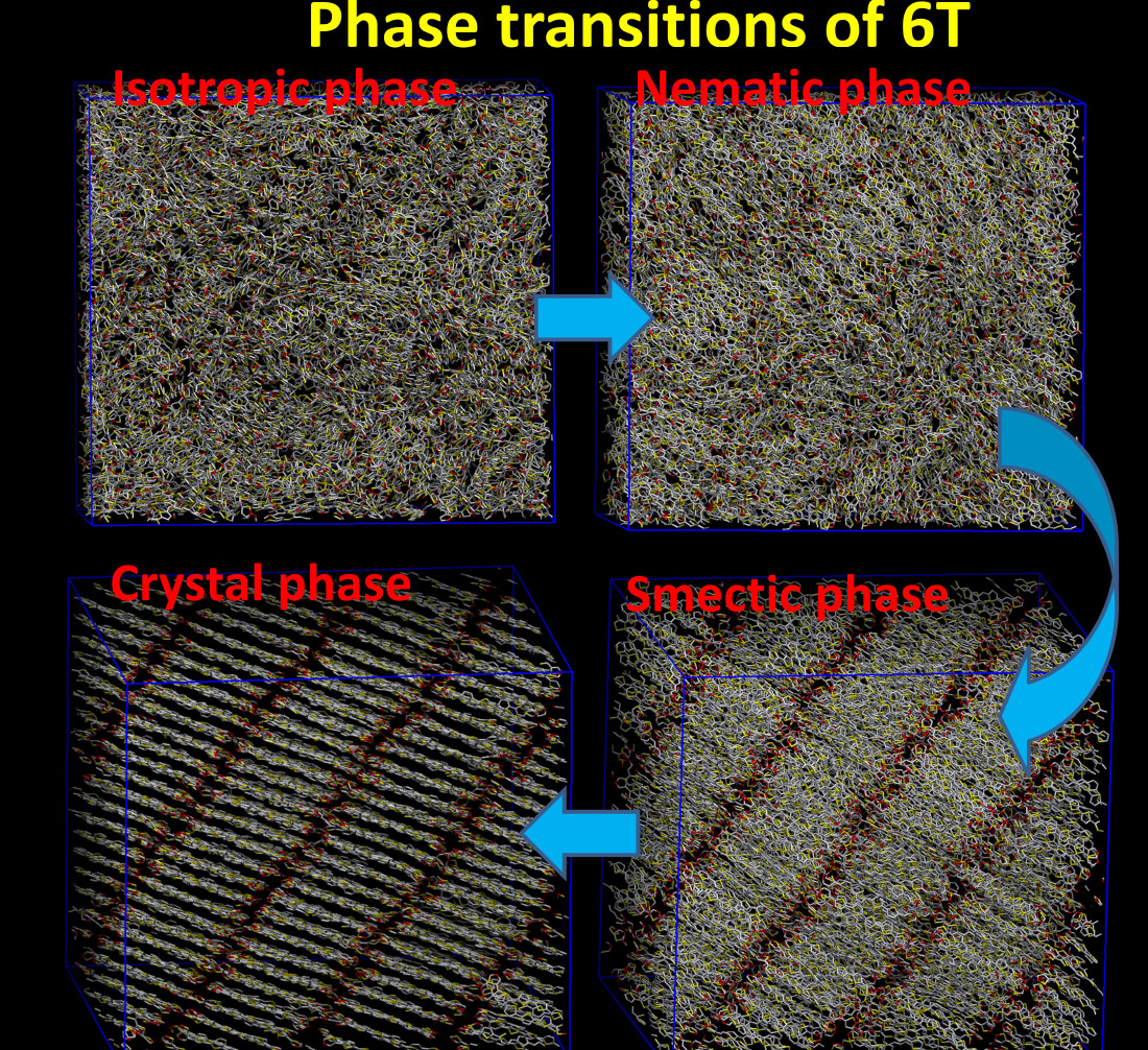
Multiscale modeling and simulation of polymer-based materials for use in microelectronics
Charge transfer in organic semiconducting polymers (which are often characterized by a π-conjugated backbone) is sensitive to conformational disorder along the main chain backbone and to chemical defects in the bulk of the material. Thus, despite intense basic research in the field for more than a decade, only few polymer-based devices for electronic transport have been realized up to now. In general, charge mobility in polymer semiconductors is strongly dependent on morphology at the molecular level but also at the level of entire chains (e.g., the chain end-to-end distance). At even larger scales, polymer semiconductors consist usually of crystalline domains separated by amorphous regions. This happens because molecules in low molecular-weight (MW) films are able to form well-ordered crystals more easily than molecules in high-MW films. Thus, to understand charge transport one needs to understand first self-assembly at the nano-scale where crystalline and amorphous domains co-exist but also close to the electrodes where chains are practically sandwiched between two metallic plates. Depending on the environmental conditions, the disordered polymer layer is also doped with ions, which further affect charge transport through the material. The motion of charge carriers in these systems, particularly between different chains, is sensitive to local ordering, and although the link between high ordering and charge mobility is well established, quite often the need to optimize chain packing comes up with additional challenges. For example, the addition of alkyl side chains (which helps improve solubility and reduce the melting temperature increases the distance between polymer chains) leads to considerably reduced charge transfer along the chain direction. Also, usually, and despite this higher local ordering in low-MW samples, higher charge mobility are observed in films of high-MW polymer semiconductors. This can be explained by the fact that longer polymer chains are able to form bridges between different crystalline domains. Using as model systems conjugated polymers that are known to form morphology at the nano-scale (e.g., two-dimensional sheets) such as P3HT, PQT, and PBTTT, in our team we develop multi-scale modelling tools addressing:
- microstructure and morphology development at the nanoscale due to self-assembly, the dominant assembling mechanisms, and the resulting supramolecular arrangement of the formed two-dimensional foils or layers
- structural properties in the crystalline and amorphous regions (such as inter-ring and ring-tail torsions, long-range correlations between the orientations of thiophene rings and their temperature dependence, radial distribution functions, interchain spacing), also between the nano-domains and how they affect the charge-transfer behavior
- the effect of regioregularity (stereo-regular versus random-regular) on the self-assembly properties of these systems and eventually on their charge-transfer behavior
- the presence of defects in the crystal structure as a function of temperature through large scale classical molecular dynamics simulations
- intra- versus inter-chain contributions to charge mobility and their dependence on torsional defects and the inter-chain (lamellae) spacing